- 您现在的位置:买卖IC网 > Sheet目录995 > NCL30100ASLDGEVB (ON Semiconductor)BOARD DEMO SGL LAYER PWM DIM LED
�� �
�
�NCL30100�
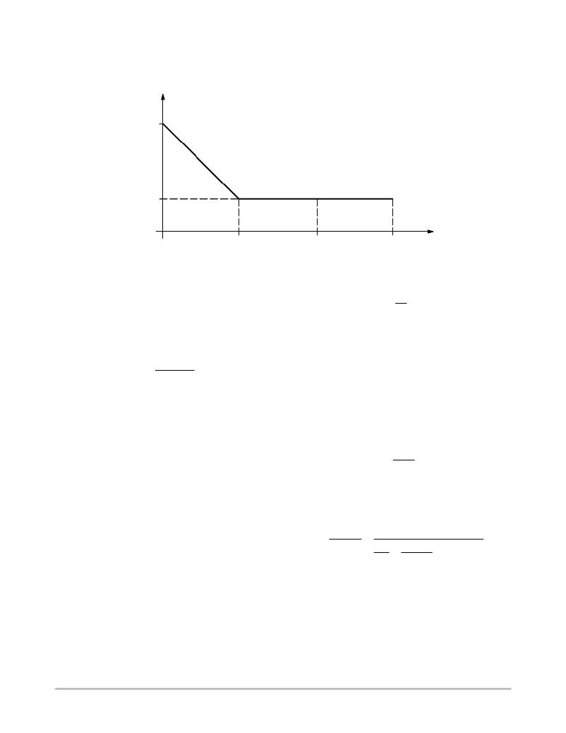
�The� current� sense� characteristic� can� be� seen� in� Figure� 22.�
�As� illustrated,� by� varied� the� IVC� current� between� 0� ?� 50� m� A,�
�the� sourcing� current� can� range� from� 12.5� to� 50� m� A.�
�V�
�50� m� A�
�12.5� m� A�
�0� m� A�
�50� m� A�
�100� m� A�
�140� m� A�
�m� A�
�IVC� Pin� Sink� Current�
�Figure� 22.� Current� Sense� Regulation� Characteristic�
�Biasing� the� controller�
�The� NCL30010� Vcc� input� can� range� up� to� 18� V.� For�
�applications� that� have� an� input� voltage� that� is� greater� than�
�t� on� +� L� @�
�I� pk�
�V� in�
�)� CS� delay�
�(eq.� 4)�
�R� 2� +�
�t� off� +� C� T� @� )� CT� delay�
�F� SW� +�
�+�
�t� on� )� t� off�
�pk�
�T�
�offset�
�)� )� 435� @� 10� ?� 9�
�50� @� 10� ?� 6�
�in�
�that� level,� an� external� resistor� should� be� connected� between�
�V� in� and� the� V� CC� supply� capacitor.� The� value� of� the� resistor�
�can� be� calculated� as� follows:�
�V� in� *� V� CC�
�(eq.� 2)�
�I� CC2�
�Where:�
�V� CC� ?� Voltage� at� which� IC� operates� (see� spec.)�
�I� CC2� –� Current� at� steady� state� operation�
�V� in� ?� Input� voltage�
�The� I� CC� current� is� composed� of� two� components:� The�
�quiescent� current� consumption� (300� m� A)� and� the� switching�
�current� consumption.� The� driver� consumption� depends� on�
�the� MOSFET� selected� and� the� switching� frequency.� Total�
�current� consumption� can� be� calculated� using� following�
�formula:�
�I� CC� +� 300� @� 10� ?� 6� )� C� MOSFET� @� V� CC� @� f� switching� (eq.� 3)�
�In� applications� where� the� input� voltage� Vin� is� varying�
�dramatically,� a� zener� can� be� used� to� limit� the� voltage� going�
�into� V� CC� ,� thus� reducing� the� switching� current� contribution.�
�Switching� Frequency�
�The� switching� frequency� varies� with� the� output� load� and�
�input� voltage.� The� highest� frequency� appears� at� highest�
�Where:�
�L� ?� Inductor� inductance�
�I� pk� ?� Peak� current�
�As� seen� from� the� above� equation,� the� turn� on� time� depends�
�on� the� input� voltage.� In� the� case� of� a� low� voltage� AC� input�
�where� there� is� ripple� due� to� the� time� varying� input� voltage�
�and� input� rectifier,� natural� frequency� dithering� is� produced�
�to� improve� the� EMI� signature� of� the� LED� driver.�
�The� turn� off� time� is� determined� by� the� charging� of� the�
�external� capacitor� connected� to� the� CT� pin.� The� minimum�
�t� off� value� can� be� computed� as:�
�V� offset�
�(eq.� 5)�
�I� CT�
�Where:�
�V� offset� ?� Offset� voltage� (see� parametric� table)�
�I� CT� ?� C� T� pin� source� current� (see� parametric� table)�
�Finally,� the� switching� frequency� then� can� be� evaluated� by:�
�1� 1� (eq.� 6)�
�L� @� I� C� @� V�
�V�
�The� sum� of� the� nominal� CS� delay� and� CT� delay� is�
�approximately� 435� nsec.�
�input� voltage.� Since� the� peak� inductor� current� is� fixed,� the�
�on� ?� time� portion� of� the� switching� period� can� be� calculated:�
�http://onsemi.com�
�10�
�发布紧急采购,3分钟左右您将得到回复。
相关PDF资料
NCL30105GEVB
BOARD EVAL 80V 350 FOR LED DRV
NCP1013LEDGEVB
BOARD EVAL 5W UNIV LED DRIVER
NCP1028LEDGEVB
EVAL BOARD FOR NCP1028LEDG
NCP1216AFORWGEVB
BOARD EVAL NCP1216A 35W
NCP1351LEDGEVB
EVAL BOARD FOR NCP1351LEDG
NCP3065BBGEVB
BOARD EVAL NCP3065 MR16 BOOST
NCP3066SCBCKGEVB
EVAL BOARD FOR NCP3066SCBCKG
NCP5005GEVB
EVAL BOARD FOR NCP5005G
相关代理商/技术参数
NCL30100SNT1G
功能描述:LED照明驱动器 LED DRIVER CONTROLLER RoHS:否 制造商:STMicroelectronics 输入电压:11.5 V to 23 V 工作频率: 最大电源电流:1.7 mA 输出电流: 最大工作温度: 安装风格:SMD/SMT 封装 / 箱体:SO-16N
NCL30105
制造商:未知厂家 制造商全称:未知厂家 功能描述:Constant Off Time PWM Current-Mode Controller for
LED Applications
NCL30105DR2G
功能描述:LED照明驱动器 Flexible Dimmable Buck LED Driver Cont RoHS:否 制造商:STMicroelectronics 输入电压:11.5 V to 23 V 工作频率: 最大电源电流:1.7 mA 输出电流: 最大工作温度: 安装风格:SMD/SMT 封装 / 箱体:SO-16N
NCL30105GEVB
功能描述:LED 照明开发工具 80V 350 MA BUCK LED Driver
RoHS:否 制造商:Fairchild Semiconductor 产品:Evaluation Kits 用于:FL7732 核心: 电源电压:120V 系列: 封装:
NCL30160
制造商:未知厂家 制造商全称:未知厂家 功能描述:1.0A Constant-Current Buck Regulator for Driving
High Power LEDs
NCL30160DR2G
功能描述:LED照明驱动器 40V LED Buck Regltr
RoHS:否 制造商:STMicroelectronics 输入电压:11.5 V to 23 V 工作频率: 最大电源电流:1.7 mA 输出电流: 最大工作温度: 安装风格:SMD/SMT 封装 / 箱体:SO-16N
NCL30160GEVB
功能描述:电源管理IC开发工具 40V, 1A LED Driver EVM
RoHS:否 制造商:Maxim Integrated 产品:Evaluation Kits 类型:Battery Management 工具用于评估:MAX17710GB 输入电压: 输出电压:1.8 V
NCL30161MNTXG
制造商:ON Semiconductor 功能描述:CONSTANT-CURRENT BUCK REG - Tape and Reel 制造商:ON Semiconductor 功能描述:Buck Reg,Constant Current,for LED Drive